12 Key Differences and Pros/Cons: SiC MOS vs. Si MOS
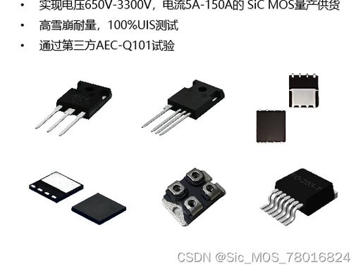
As a core switching device of the third-generation wide-bandgap semiconductor, SiC MOSFETs leverage intrinsic material advantages to significantly outperform traditional silicon-based MOSFETs (Si MOS) in high-voltage, high-frequency, and high-temperature power conversion applications.
SiC MOSFETs, as the core switching devices of third-generation wide-bandgap semiconductors, leverage intrinsic material advantages to significantly outperform traditional silicon-based MOSFETs (Si MOS) in high-voltage, high-frequency, and high-temperature power conversion applications. While both are unipolar voltage-driven MOS devices, they differ fundamentally in material composition, static conduction, dynamic switching, high-temperature performance, drive design, body diode behavior, package power density, and total system cost. This article systematically compares SiC MOS and Si MOS across 12 key dimensions, addressing critical selection criteria for hardware engineers, power topology design, and core concerns in automotive and photovoltaic applications.
01 Differences in underlying material and device architecture
Intrinsic physical parameters of silicon (Si) and silicon carbide (SiC) determine the performance ceilings of their respective MOS devices. Key parameter differences are as follows:
Breakdown electric fieldThe breakdown field strength of SiC is 10 times that of silicon (3.26MV/cm vs. 0.3MV/cm), enabling equivalent voltage ratings with an extremely thin drift layer. To increase the voltage rating of silicon devices, the drift region must be thickened, causing the on-resistance to rise sharply by a factor of 2 to 2.5.
Bandgap: SiC bandgap is 3 eV, while silicon is only 1.12eV. At high temperatures, SiC exhibits extremely low leakage current, whereas silicon devices experience significant leakage degradation above 150°C.
Thermal ConductivityThe thermal conductivity of SiC is 4~5 times that of silicon, enabling more efficient heat dissipation and significantly simplifying the cooling system.
electron saturation drift velocity: SiC has faster electron mobility and natively supports nanosecond-level high-speed switching.
Structural Level:
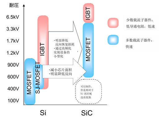
Si MOS: High-voltage models above 600V rely on Super Junction (SJ) structures to mitigate on-resistance, yet chip area remains large at high voltages. For scenarios exceeding 900V, Si MOS devices have little practical value; higher-loss Si IGBTs must be used instead.
SiC MOS: Achieves low impedance across the full 650V–3300V voltage range using a unipolar MOS structure without conductivity modulation. Unlike IGBTs, it eliminates tail current caused by minority carrier accumulation, making it perfectly compatible with high-voltage, high-frequency applications.
Comparison of 02 On-Resistance (Rdson) and Die Area
On-resistance is a core loss metric for power devices. SiC offers a dominant advantage over competing technologies at the same voltage rating:
900V-class devices achieve the same on-resistance with SiC MOS chip areas of only 1/35 that of standard Si MOS and 1/10 that of Super Junction (SJ) MOS.
Same package and voltage rating: SiC Rds(on) is significantly lower than silicon MOSFETs; even small-footprint SiC can replace larger silicon MOSFETs.
Smaller chip sizes deliver two key benefits: reduced gate charge (Qg) and lower junction capacitances (Ciss/Coss), further cutting switching losses.
Shortcomings comparison: Silicon MOS offers higher channel mobility and lower conduction cost in low-voltage scenarios (≤200V), with no advantage for SiC; only above 600V does SiC demonstrate comprehensive superiority in high-voltage conduction performance.
03 High-Temperature RDS(ON) Thermal Characteristics (Key Differences in Thermal Design)
High-temperature operation is a core challenge for both vehicle-mounted and outdoor industrial power supplies, with vastly different temperature sensitivities between the two:
Silicon MOSAt a junction temperature of 150°C, the on-resistance increases to more than 2 times its value at room temperature (25°C). Under full-load high-temperature conditions, conduction losses double, leading to intensified heating and a vicious cycle. Conventional silicon MOSFETs have a maximum safe junction temperature of only 150°C.
SiC MOSThe on-resistance increases gradually with temperature; at a rated junction temperature of 175°C, Rdson rises by less than 50%. Certain automotive-grade SiC devices can withstand short-term operation at 200°C. Under high-temperature full-load conditions, the increase in conduction loss is minimal, significantly reducing heatsink size and weight.
Real-world performance: For high-temperature equipment like sealed in-vehicle electronic controls and outdoor PV inverters, Si MOSFETs require heavy water or air cooling. SiC allows a lightweight aluminum substrate, boosting system power density by over 20%.
04 Gate Drive Voltage Requirement Mismatch (Most Common Design Pitfall)
The two channels operate on different conduction mechanisms, so their driving voltage windows cannot be directly reused:
Silicon MOS Drive Solution
The standard universal drive voltage is Vgs=10~15V. A stable, false-trigger-free operation is achieved simply by setting 0V for turn-off. With high channel mobility, a 12V drive is sufficient to reach the specified minimum Rdson. The driver circuit is simple and the solution is mature.
Hard Requirements for SiC MOS Driver
We recommend setting Vgs to approximately +18V. If only standard Si MOSFETs are driven with 10~15V, the channel resistance will not be sufficiently reduced, causing Rdson to spike significantly and creating a risk of thermal runaway under sustained full load.
During the turn-off phase, a negative voltage of -3V~-5V is recommended: SiC threshold voltages are only 2~3V and decrease further at high temperatures. Miller coupling from high-speed switching can easily cause false turn-on and device failure. This is not required for silicon MOSFETs.
Lower drive power: SiC devices have lower Qg, resulting in reduced driver chip power consumption compared to silicon MOSFETs at the same current rating. However, they require stricter matching of parasitic inductance and gate resistance in the drive circuit.
05 Vg-Id Threshold and Anti-Interference Characteristics
Silicon MOS: The threshold voltage is typically 4~5V, providing a large noise margin. It resists false triggering even with standard drive circuits and long wiring.
SiC MOSThe room-temperature threshold is only 2.5~3V. The threshold is defined under a small current of a few mA, while conduction at high currents requires a gate voltage above 8V. Fast switching generates extremely high dv/dt, making the top and bottom switches in a bridge topology highly susceptible to crosstalk. Without negative-voltage turn-off, its noise immunity is weaker than silicon MOSFETs. PCB layout optimization for gate traces and proper gate resistor matching are essential.
06 Enable Turn-On Loss and Body Diode Recovery Loss
For inductive loads, turn-on loss is primarily determined by the reverse recovery current of the freewheeling diode, with a significant difference between the two.
The intrinsic body diode of a silicon MOSFET is a standard PN junction, which suffers from significant minority carrier accumulation. This results in high peak reverse recovery current and long recovery time. At elevated temperatures, recovery losses are further exacerbated, necessitating the external addition of Si fast recovery diodes (FRDs) for high-power LLC and inverter circuits.
The SiC MOS body diode has an extremely short minority carrier lifetime, delivering ultra-fast recovery characteristics comparable to a SiC Schottky barrier diode (SBD) in the tens of nanoseconds range. Its reverse recovery loss is only 1/10~1/30 that of a silicon body diode, eliminating the need for an external freewheeling diode and reducing both component count and wiring losses.
Switching speed is determined by the external gate resistor (Rg): Silicon MOSFETs typically use 10–50Ω, while SiC devices recommend a low gate resistance of 2–10Ω for fast turn-on, paired with an RC snubber to suppress voltage spikes.
07 Turn-Off Loss and High-Frequency Limit
This is the core performance advantage of SiC MOSFETs, representing a bottleneck that silicon MOSFETs cannot overcome.
Silicon MOS: Although it lacks the tail current of bipolar IGBTs, its large junction capacitance and prolonged turn-off transition cause switching losses to rise exponentially with frequency. The maximum stable operating frequency for commercial silicon MOSFETs is only 20~10 kHz; beyond this limit, overall system efficiency drops sharply.
SiC MOS: Pure unipolar devices exhibit no tail current; turn-off loss (Eoff) is reduced by 70%~90% compared to equivalent-voltage Si MOSFETs and remains stable across temperature. They can reliably operate at high frequencies from 50 kHz to 500 kHz.
Higher switching frequency delivers system benefits: increasing the frequency by 3 to 10 times reduces the volume of passive components like transformers, inductors, and filter capacitors by over 50%, significantly achieving overall device miniaturization and weight reduction.
08 Internal Gate Resistance and Gate Charge Characteristics
Silicon MOS: Thick drift region and large chip area result in low internal gate resistance, higher total gate charge (Qg), elevated Miller charge (Qgd), and a flatter Miller plateau.
SiC MOSFETs feature significantly smaller chip sizes than silicon MOSFETs at the same current rating. They exhibit higher internal gate resistance but lower total gate charge (Qg) and Miller charge (Qgd). During high-speed switching, the narrow Miller plateau leads to rapid dv/dt transitions, increasing electromagnetic interference (EMI). Proper gate resistor selection is essential to balance power losses with EMI noise.
09 Body Diode Forward Voltage Drop Vf and Reverse Conduction Solution
Silicon MOS body diode
Silicon has a narrow bandgap, with a PN junction turn-on voltage of approximately 0.7V and low forward voltage drop. However, it exhibits poor reverse recovery characteristics. In bridge topologies, relying solely on the internal body diode for freewheeling results in extremely high losses. A series blocking diode is required to prevent current backflow, which increases conduction losses and material costs.
SiC MOSFET body diode
Intrinsic Defect: Due to SiC's wide bandgap, the body diode has an on-voltage of approximately 3V and a very high forward voltage drop (Vf), resulting in significant conduction losses during the dead time.
Optimized Solution: In inverter/LLC circuits, turn on the MOSFET gate early after dead time. This allows conduction through the reverse MOS channel, bypassing the body diode. The body diode is used only briefly during dead time, completely eliminating the disadvantage of high forward voltage drop (Vf).
System Advantages: When paralleling external SiC SBDs, the body diode's Vf is significantly higher than that of Schottky diodes, eliminating the need for an additional low-voltage blocking diode in series and simplifying the peripheral circuitry.
10 encapsulation adaptation and power density performance
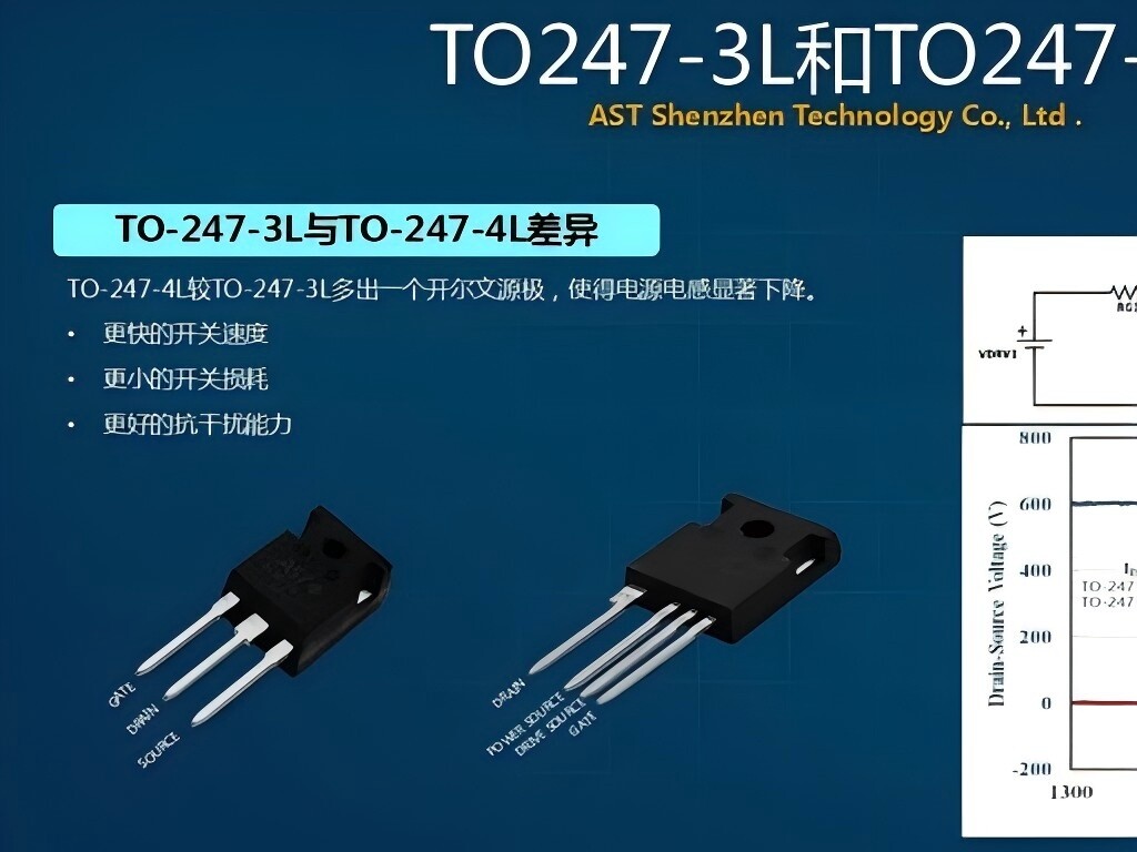
1. Silicon MOSFor the same power and voltage rating, chip area is larger, leading to the use of large-volume TO247 and TO220 packages. With multiple chips inside the module, power density remains low. Additionally, standard TO247-3L packaging exhibits slower switching speeds and weaker noise immunity compared to Kelvin Source 4L packaging.
SiC MOS: Chip miniaturization enables small packages to handle high currents, making TO252 and TO247-4L Kelvin packages the industry standard. Kelvin source separation for drive and power loops significantly reduces gate oscillation and switching losses. Compared to silicon-based solutions, system volume is reduced by 30%~50% at the same power rating. SiC power modules are widely adopted in new energy vehicle OBCs and main inverters.
11 Use Case Segmentation (Core Selection Reference)
When to choose silicon MOS: preferred option
Low-voltage operation: ≤400V for consumer power supplies, chargers, and low-voltage DC-DC converters;
Low-frequency, low-power: ≤20 kHz adapters, small-power Buck/Boost.
Cost-sensitive low-end devices: No need for miniaturization; ample thermal headroom.
No extreme high-temperature environments; extremely low batch cost requirements.
SiC MOS Irreplaceable Scenarios (Prioritize SiC)
High-voltage platform: 650V/1200V photovoltaic inverters, energy storage PCS, and EV chargers.
High Frequency & High Density: LLC Resonant Power Supplies, High-Density Power for AI Servers
In-vehicle high-temperature scenarios: new energy main drive inverters, on-board chargers (OBC), and DC/DC converters.
Industrial high-voltage drives, rail transit, and aerospace high-temperature power systems.
Cost and Reliability Gaps: 12
Silicon MOS
Advantages: Mature supply chain, low wafer cost, universal drive solutions, wide spare parts selection, and strong resistance to voltage surges.
Drawbacks: High switching losses at high voltage and frequency, poor performance at elevated temperatures, high costs for system-level thermal management and passive components, and significantly higher energy consumption costs over long-term operation.
SiC MOS
Advantages: Low total system cost (heat dissipation, magnetic components, and reduced chassis size offset component price differences), significant long-term energy efficiency gains, and high-temperature/high-voltage resilience.
Limitations: Higher per-unit cost than silicon MOSFETs, complex gate driver design, high crystal brittleness, and poor resistance to lightning strikes or voltage spikes. RC snubbers and voltage clamping protection circuits are required.
Summary
SiC MOSFETs are not a simple upgrade of silicon MOSFETs; they represent a breakthrough across performance dimensions enabled by third-generation wide bandgap materials. In high-voltage (> 600V), high-frequency, and high-power applications operating at elevated temperatures, SiC devices gradually replace superjunction MOSFETs and silicon IGBTs due to their lower conduction and switching losses, higher power density, and superior high-temperature stability. However, in low-voltage, low-frequency, and ultra-low-cost consumer scenarios, silicon MOSFETs remain unmatched in cost-performance ratio.
When selecting hardware, do not rely solely on the price of individual components. Evaluate system-level total cost by considering switching frequency, operating temperature, overall thermal management, passive component footprint, and long-term energy consumption to determine whether SiC MOS or silicon MOS is better suited for your product requirements.
Tags: #SiC_MOS #Power_Hardware #Component_Selection #New_Energy_Vehicles #PV_Storage